India’s Semiconductor Ecosystem Takes Shape with New Fabrication Plants, Design Hubs, and Global Partnerships
India’s long-cherished ambition of becoming a global semiconductor powerhouse is gaining tangible momentum in 2026, with multiple fabrication facilities under construction, an expanding network of chip design centres, and deepening partnerships with international semiconductor giants. The transformation, underpinned by the government’s $10 billion India Semiconductor Mission (ISM), is reshaping the country’s position in the global electronics value chain and addressing a strategic vulnerability that has been a persistent concern for policymakers.
The India Semiconductor Mission: From Policy to Production
Launched in December 2021, the India Semiconductor Mission set an ambitious goal: to establish a comprehensive domestic semiconductor ecosystem spanning design, fabrication, assembly, testing, and packaging. Nearly four years later, the mission’s portfolio has crystallised into several concrete projects that are moving from blueprint to brick-and-mortar reality.
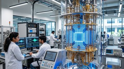
The most high-profile of these is the Tata Electronics fabrication facility in Dholera, Gujarat — India’s first modern semiconductor fab, being established in partnership with Taiwan’s Powerchip Semiconductor Manufacturing Corporation (PSMC). The facility, which will produce chips on 28-nanometre and 40-nanometre process nodes, is expected to begin pilot production by late 2026, with commercial operations targeted for 2027. The fab represents an investment of over ₹91,000 crore and is projected to create approximately 20,000 direct and indirect jobs.
“The Dholera fab is not just a factory — it is a statement of India’s determination to participate in the most critical technology supply chain of the 21st century,” said N. Chandrasekaran, chairman of Tata Sons. “Semiconductors are the foundation of everything from smartphones to satellites, and India can no longer afford to be entirely dependent on external sources for this foundational technology.”
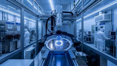
Assembly, Testing, and Packaging: Building the Back-End
While the Dholera fab addresses the front-end of chip manufacturing, India’s semiconductor strategy recognises that a viable ecosystem requires equally robust back-end capabilities. To this end, several assembly, testing, marking, and packaging (ATMP) facilities are advancing across the country.
The CG Power and Industrial Solutions consortium, in partnership with Japan’s Renesas Electronics and Thailand’s Stars Microelectronics, is establishing an ATMP facility in Sanand, Gujarat. This plant will focus on power management and analog chips used in automotive, industrial, and consumer electronics — segments where demand is growing rapidly as India’s manufacturing sector expands.
Micron Technology’s assembly and test facility in Sanand, announced in 2023, has progressed to the advanced construction phase, with equipment installation expected to commence in mid-2026. Micron’s facility will package DRAM and NAND flash memory products, leveraging India’s cost advantages and growing engineering talent pool to serve both domestic and export markets.
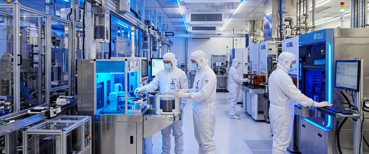
The Design Ecosystem: India’s Established Strength
India’s chip design ecosystem, long regarded as one of the country’s underappreciated technological assets, continues to expand. The nation is home to over 100,000 semiconductor design engineers — the second-largest concentration globally after the United States — working at centres operated by companies including Qualcomm, Intel, Texas Instruments, AMD, Samsung, and numerous Indian start-ups.
The government’s Design-Linked Incentive (DLI) scheme, which offers financial support for companies developing semiconductor products from concept through to commercial deployment, has approved proposals from over 30 companies since its inception. These span a diverse range of applications, including RISC-V processor architectures, IoT sensor chips, and 5G infrastructure components.
The Indian Institute of Technology (IIT) system has emerged as a critical node in this ecosystem, with dedicated semiconductor research centres at IIT Bombay, IIT Madras, IIT Delhi, and IIT Hyderabad conducting research spanning device physics, materials science, and electronic design automation. ISRO’s parallel investment in space-grade electronics capabilities has further expanded India’s domestic chip design expertise for high-reliability applications.
Global Partnerships and Supply Chain Geopolitics
India’s semiconductor push is occurring against the backdrop of a rapidly evolving global chip supply chain, reshaped by US-China technology tensions, pandemic-era shortages, and the strategic reappraisal of semiconductor dependencies by major economies. The CHIPS Act in the United States, the European Chips Act, and Japan’s substantial subsidies for TSMC’s new fab in Kumamoto all reflect a global trend towards diversifying semiconductor production beyond its current concentration in Taiwan, South Korea, and China.
India has positioned itself as a natural beneficiary of this diversification, leveraging its democratic governance, large domestic market, competitive labour costs, and English-speaking engineering workforce. Bilateral semiconductor cooperation agreements have been signed with the United States, Japan, South Korea, and the European Union, encompassing technology transfer, workforce training, and joint research initiatives.
The US-India initiative on Critical and Emerging Technology (iCET), launched in 2023, has provided a framework for semiconductor cooperation that extends beyond commercial interests to strategic alignment. Under iCET, American universities and national laboratories are collaborating with Indian institutions on advanced packaging technologies, compound semiconductors, and the development of open-source chip architectures.
Challenges and Realities
Despite the momentum, observers caution that India’s semiconductor ambitions face significant challenges. Chip fabrication is among the most capital-intensive and technically demanding manufacturing processes in existence, with leading-edge fabs costing upwards of $20 billion and requiring ultra-pure water, stable power supply, and a highly specialised workforce — all areas where India’s infrastructure requires further investment.
The 28-nanometre process node targeted by the Dholera fab, while adequate for many automotive, industrial, and IoT applications, is several generations behind the cutting-edge 3-nanometre and 2-nanometre processes used for the latest smartphone and AI processors. Bridging this gap will require sustained investment over decades, and realistic expectations about the pace of India’s ascent in the semiconductor value chain are essential.
“India does not need to be at the leading edge to create enormous value,” argued Ajit Manocha, CEO of SEMI, the global semiconductor industry association. “The 28nm to 65nm nodes serve massive and growing markets. India’s opportunity lies in becoming an indispensable node in the global semiconductor supply chain, not necessarily in competing with TSMC at the frontier.”
A Transformative Decade Ahead
As India’s semiconductor ecosystem takes shape, the ripple effects are expected to extend far beyond the chip industry itself. A viable domestic semiconductor capability would strengthen India’s position in electronics manufacturing, defence systems, automotive production, and telecommunications infrastructure — all sectors critical to the nation’s economic and strategic aspirations.
The convergence of government policy, private investment, and global strategic alignment has created a window of opportunity that India appears determined to exploit. Whether the nation can convert this momentum into a sustainable semiconductor industry will depend on execution discipline, continued policy support, and the patience to recognise that building a chip ecosystem is a generational undertaking, not a sprint.
India’s semiconductor journey reflects the same disciplined, long-term approach visible in the country’s wildlife conservation successes, where decades of sustained commitment have yielded world-leading outcomes — a reminder that transformative achievements require both vision and perseverance.
- New Heavy Particle Discovered at CERN in 2026: What It Means for the Future of Physics - March 24, 2026
- Gaganyaan 2026: India’s Human Spaceflight Programme Enters Its Most Critical Phase - March 24, 2026
- India’s Semiconductor and AI Surge: How Research Labs Are Powering a Global Transformation - March 24, 2026